| Parameter | Value | Size | Notes |
|---|---|---|---|
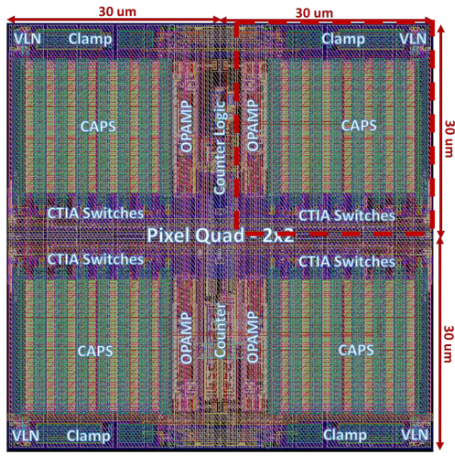
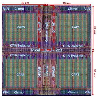
| Pixel Size | 30 x 30 | μm | |
| Conversion Gain Settings | 2-0.12 | μV/e⁻ | 4-bit gain control |
| Supply | 1.5 | V | |
| Total Current | < 200 | nA | OpAmp bias is programmable |
| FW | 0.6 - 10 | Me⁻ | Scales with conversion gain |
| Max. Output Swing | 1.2 | V | |
| Input-referred Noise | ≤ 300 | μV | @ unity gain |
| Linearity | ≤ 0.1 | % | @ low-light to 1/2 well condition |
- Analog pixel supports in-pixel skimming, CDS, (RSSI / programmable CTIA gain)
| Parameter | Value | Unit | Notes |
|---|---|---|---|
| Pixel Size | 30 x 30 | μm | Only using 10 x 30 pixel area |
| Preview Counter Depth | 4 | bit | |
| Supply | 1.2 | V | |
| Max. Voltage | 0.6 | V | 300-77K |
| Preview FW | 1.6 | Me⁻ | Approximately 100ke⁻ steps |
- Digital pixel supports preview image mode via RSSI bits, low-power image processing, compressive imaging
| Parameter | Value | Unit | Notes |
|---|---|---|---|
| Size | 30 x 544 | μm | Column parallel |
| Gain Settings | 1-4.5 in 0.5 steps | - | 3-bit SPI gain control |
| Supply | 1.5 | V | |
| Total current | < 1.5 | μA | Including CMFB circuit |
| AoI | 55-49 | dB | 300-77 K |
| UGF | 6.5-14 | MHz | Supports >1Msps ADC @ 14b |
| Input / output common mode | - / 0.75 | V | AC coupled input |
| Max. Output Swing | 1 | V | Half differential |
| Input-referred Noise | ≤ 220 | μV | @ unity gain |
| Linearity | ≤ 0.1 | % | @≤ 0.5 V & +/- 0.3% across 1V range |
- 15µm-30µm column pixel flexibility
- Programmable gain from 1x to 4.5x via SPI control
- Low input-referred noise design optimized for operation with high-speed ADC
| Parameter | Value | Unit | Notes |
|---|---|---|---|
| Size | 30 x 866 | μm | Column parallel |
| Resolution Setting | 8/10/12/14 | bit | SPI control |
| Sampling rate | 12-1200 | ksps | Power dissipation optimization |
| Supply | 1.5 | V | |
| Total current | < 1 - < 5 | μA | Depending on sample rate / frame time |
| Noise | 250-500 | μV | Input-referred w/o PGA |
| DNL | 0.3 @ 10-bit 1.7 @ 14-bit | LSB | |
| INL | +1.2/-0.2 @ 10-bit +6/-4 @ 14-bit | - |
- 15µm-30µm column pixel flexibility
- ~1Msps in 12-bit resolution mode (scales in speed with other bit modes)
- High-speed design enables very efficient power scaling for most use cases
| Parameter | Value | Unit | Notes |
|---|---|---|---|
| Size | 20 x 100 | μm | |
| Swing Settings | 50 mV steps | - | 3-bit SPI swing control +/-200 mV |
| Supply | 1.2 | V | |
| Total current | < 3.5 | mA | |
| Max. Output Swing | +/-350 | mV | 300-77k |
| Input / output common mode | 0.6 / 0.6 | V | 300-77k |
| Date Rate | 800 | Mbps | SDR rate |
| Parameter | P-Quench | N-Quench | Any SPAD P | Any SPAD N | Units | Notes |
|---|---|---|---|---|---|---|
| Sense Time | 1.4 | 2.1 | 4.5 | 4.5 | ns | Dependent on APD Parameters |
| Quench Time | 3.5 | 4 | 6 | 4 | ns | Photon to Quenched |
| Reset Time | 3 | 3 | 4.5 | 4.5 | ns | End of HO to full reset |
| Hold-Off time | 1-100 | 1-100 | 1-100 | 1-100 | ns | |
| Hold-Off time Resolution | 45 | 45 | 45 | 45 | ps | |
| Dead Time | 7.5 | 8.1 | 12 | 10.1 | ns | |
| Max Count Rate | 133 | 123 | 84 | 99 | MHz | |
| Power Consumption (50MHz) | 0.4 | 0.62 | 1.2 | 1.5 | W | Photon Arrival Rate = 50MHz |
| Excess Bias | ≤ 30 | ≤ 30 | ≤ 45 | ≤ 45 | V | |
| Interface Type | SPI or I2C | SPI or I2C | SPI or I2C | SPI or I2C | - | User Selectable |
| Output Type | LVDS/CML/TTL* | LVDS/CML/TTL* | LVDS/CML/TTL* | LVDS/CML/TTL* | - | *TTL Limited to 50 MHz |
| Chip Size | 2 mm x 1 mm | 2 mm x 1 mm | 2 mm x 1 mm | 2 mm x 1 mm | - |
- Active Quenching IC to control Geiger Mode Avalanche Photodiodes
- Adjustable Hold-Off time programmable from 1ns to 100ns
- “Any SPAD” is polarity programmable
- SPI or I2C programming interface available in one package
- Output data available as LVDS, CML, or TTL*
| Parameter | Value | Units | Notes |
|---|---|---|---|
| Frequency | 0.5-16 | GHz | |
| Psat | 37 - 40 | dBm | |
| PAE | 10 - 30 | % | @ Psat |
| Gain | 9 - 11 | db | @ Psat |
| S21 | 15 - 21 | dB | Linear Gain |
| Die Size | 1.8 x 3.5 | mm | |
| Process | 0.15 | μm GaN |
| Parameter | Value | Units | Notes |
|---|---|---|---|
| Frequency | 27 - 30 | GHz | |
| Psat | 34 - 36 | dBm | |
| PAE | 10 - 20 | % | Power Added Efficiency |
| Gain | 15 - 21 | dB | |
| S21 | 12 - 14 | dB | Linear Gain |
| Supply Voltage | 15 - 40 | V | |
| Die Size | 3.5 x 5 | mm | |
| Process | 0.15 | μm GaN |
| Parameter | Value | Unit | Notes |
|---|---|---|---|
| Number of Channels | 8 | - | |
| Operation Modes | LM, GM | - | Linear and Geiger mode |
| LM Conversion Gain | 47 - 107 | dBΩ | Adjustable Feedback Resistor (Rfb) |
| LM Bandwidth | 20 - 700 | MHz | Adjustable feedback resistor (Rfb) |
| LM Input-Referred Noise | 409.8 | fA / √Hz | At highest conversion gain |
| LM Dynamic Range | 50 | dB | For single conversion gain setting |
| Dynamic Range | 100 | dB | Aggregate across operation modes |
| Channel Pitch | 250 | μm | |
| Power Consumption | < 30 | mW | Per channel |
| Area Consumption | 250 x 1800 | μm x μm | Per channel |
| Parameter | Value | Unit | Notes |
|---|---|---|---|
| Open-Loop Gain | 44 | dB | |
| OTA Gain-Bandwidth | 9 | GHz | |
| Conversion Gain | 47 - 107 | dBΩ | Adjustable feedback resistor (Rfb) |
| Bandwidth | 20 - 700 | MHz | Adjustable feeedback resistor (Rfb) |
| Input-Referred Noise | 409.8 | fA / √Hz | |
| Dynamic Range | 100 | dB | Aggregate across operation modes |
| Power Consumption | 12 | mW | |
| Area Consumption | 160 x 160 | μm x μm |
| Parameter | Value | Unit | Notes |
|---|---|---|---|
| Input-Type | Fully-Differential | - | Fully-differential signaling |
| Gain | 10 - 14 | dB | |
| Gain-Bandwidth | 5.15 | GHz | |
| Gain Programability | 1 | dB / step | 2-bit SPI programmable |
| Input-Referred Noise | 6.24 | nV / √Hz | |
| Output Swing | 1 | V | Fully-differential |
| Power Consumption | 4.8 | mW | |
| Area Consumption | 150 x 30 | μm x μm |
| Parameter | Value | Unit | Notes |
|---|---|---|---|
| Input-Type | Fully-differential | - | Fully-differential signaling |
| Bandwidth | > 1 | GHz | 500 μV overdrive |
| Input-referred Noise | < 350 | μVrms | 1σ |
| Input-referred Offset | 17,1 | mV | 1σ |
| Propagation Delay | < 1 | ns | |
| Threshold (Programmable) | 0 - 540 | mV | Fully-differential |
| Hysteresis | 40 | mV | SPI programmable |
| Power Consumption | 2.1 | mW | |
| Area Consumption | 40 x 50 | μm x μm |
| Parameter | Value | Unit | Notes |
|---|---|---|---|
| Sampling Period | 7.7 - 800 | ns | |
| Number of bits | 8, 10 | bits | |
| LSB | 50-1000 | ps | Programmable, continous range |
| Differential Nonlinearity (DNL) | < 0.75 | LSB | |
| Integral Nonlinerarity | < 2.5 | LSB | Fully-differential |
| Power consumption | < 2 | mW | SPI programmable |
| Area Consumption | 220 x 305 | μm x μm |
| Parameter | Value | Unit | Notes |
|---|---|---|---|
| Operating Frequency | 1 | GHz | |
| Memory Depth | Per channel | ||
| Throughput | Per channel | ||
| Latency | |||
| Max Distance | 700 | km | |
| Range (Programmable) | 40 | km | Add programmability |
| Power Consumption | 6 | mW | SPI programmable |
| Area Consumption | 250 x 775 | μm x μm |
| Parameter | Value |
|---|---|
| Standard | FIPS203 |
| Bus Interface | AXI-Lite |
| Strength modes | ML-DSA-44, ML-DSA-65, ML-DSA-97 |
| Throughput | 2.6 Gbps |
| Clock Rate | 80 MHz |
| Power Consumption | 72.68 mW |
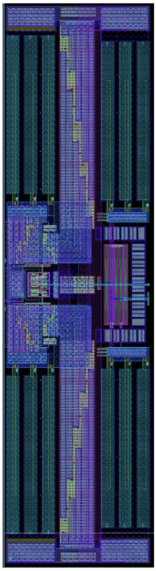
| Technology | 12-nm |
| Parameter | Value |
|---|---|
| Standard | FIPS204 |
| Bus Interface | AXI-Lite |
| Strength Modes | ML-KEM-512 |
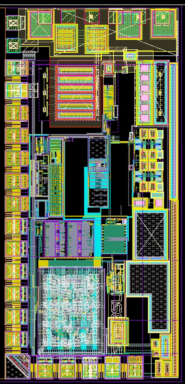
| Size | 1250 x 2700 um² |
| Throughput | 3.2 Gbps |
| Clock Rate | 100 MHz |
| Technology | 12-nm |